


Heidelberg Instruments
| |

NanoFrazor – A Nanolithography Tool for 2D & 3D devices
September 23rd, 2021
16:00 - 17:30
Faculty of Civil and Industrial Engineering - Sapienza University of Rome
ABSTRACT
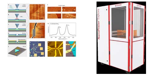
NanoFrazor lithography systems were developed as a first true alternative or extension to standard mask-less nanolithography methods like electron beam lithography (EBL). In contrast to EBL they are based on thermal scanning probe lithography (t-SPL). Here a heatable ultra-sharp probe tip with an apex of a few nm is used for patterning and simultaneously inspecting complex nanostructures. The heat impact from the probe on a thermal responsive resist generates those high-resolution nanostructures. The patterning depth of each individual pixel can be controlled with better than 1 nm precision using an integrated in-situ metrology method. Furthermore, the inherent imaging capability of the Nanofrazor technology allows for markerless overlay, which has been achieved with sub-5 nm accuracy as well as it supports stitching layout sections together with < 10 nm error. Pattern transfer from such resist features below 10 nm resolution were demonstrated.
The application range for this new nanolithography technique is very broad. The presentation will include examples for (i) high-quality metal contacting of 2D materials, (ii) tuning photonic molecules, (iii) generating nanofluidic devices and (iv) generating spintronic circuits. Some of these applications have been enabled only due to the various unique capabilities of NanoFrazor lithography like the absence of damage from a charged particle beam.
SPEAKERS:
Dr. Nils GOEDECKE, Heidelberg Instruments Nano AG
Nils Goedecke is a trained biophysicist with a PhD in Analytical Chemistry from Imperial College London, where he applied laser based direct-write lithography for microfluidics in the group of Andreas Manz. After his PhD in 2003, he was a Postdoc in the BioMEMS Laboratory at MIT. In 2005, he moved to Zurich where he was appointed team leader for microfluidics and senior researcher at ETH Zurich. In 2012, he became group leader at the Biomechanics Lab at the University Hospital where he was responsible for the in-house microfabrication facility until 2017. From 2010 to early 2018, Nils ran his own startup company Microduits.
At Heidelberg Instruments Nano, Nils Goedecke is part of the sales team, responsible to identify and consult future customers, who would benefit from nanopatterning with our NanoFrazor systems.